Date of Writeup: 2026-03-18
https://swordofsecrets.comThis writeup reflects where we actually are now. We are past basic identification. We have a live serial path, confirmed external flash contents, and a command flow that advances the puzzle. This is still discovery work, but it is no longer blind guessing.
We have confirmed live interaction with the device over serial. The board accepts framed commands, pulls in small blocks of data, and reaches a real SOLVE path when given the right sequence.
The sparse external flash contents line up with what the UART text references, especially the first region at 0x10000.
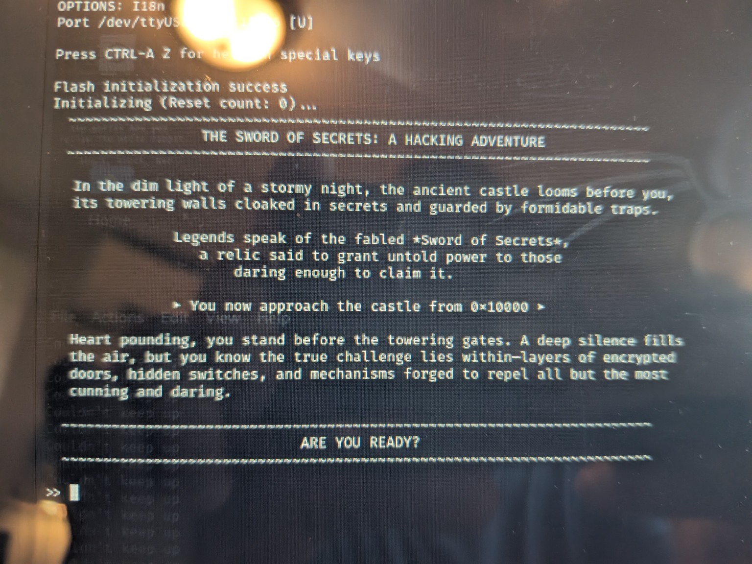
The board presents a serial console that prints the story text and prompt. This is the interface that matters right now. We are getting actual progression here, not just a banner.
Flash initialization success
Initializing (Reset count: 0)...

THE SWORD OF SECRETS! A HACKING ADVENTURE

You now approach the castle from 0x10000
>>
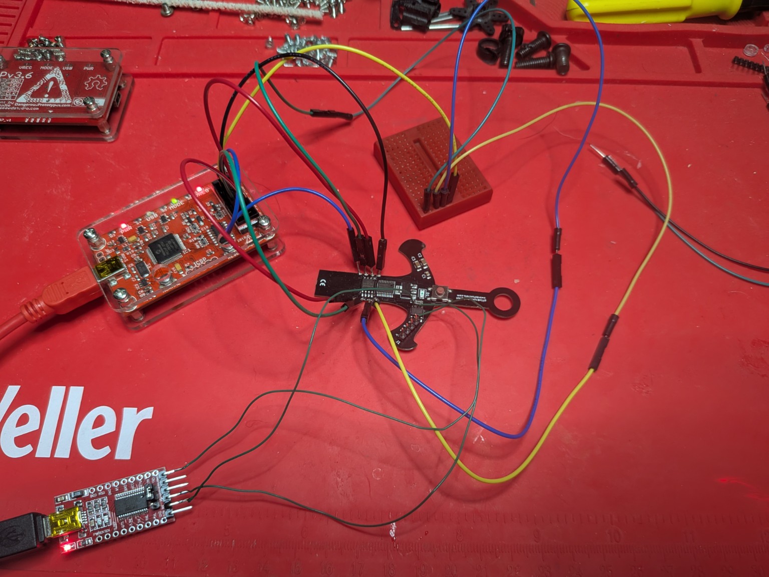
We originally treated this as a straight UART job using the serial adapter, which was correct for talking to the console. It is also worth stating clearly now that the board has a CH340N on it, so USB itself can also be used for serial access. In other words, serial can be reached either from the adapter on the serial pins or through the board's own USB path.
One important early find was that not every header on the board is a serial header. The 4 pin header is the CH32V003 debug path. It is single wire debug, not a second serial console. We got to that conclusion by lining up the board parts with the expected roles. The CH340N explains the USB serial side. The CH32V003 explains the SWIO side.
SWIO / RST / GND / 3.3V
So the practical split is simple. Use serial for gameplay and command interaction. Use SWIO later for MCU level inspection once the correct WCH capable tool is in hand.
The Winbond chip identifies correctly and was later dumped cleanly off board. The full chip is mostly erased, but a few tiny programmed regions exist and those are clearly intentional. We first suspected the flash mattered because the prompt itself points to an address. That gave us something concrete to compare against.
JEDEC ID
0xEF 0x40 0x18

Interesting programmed regions
0x010000
0x020000
0x030000
0x040000
The strongest example is the first programmed region matching the UART text.
You now approach the castle from 0x10000
That made the flash feel less like generic storage and more like challenge material tied to progression.
The board wants command groups, not random text. We did not get traction by throwing arbitrary input at it. What finally mattered was recognizing the repeated framed structure in the traffic and replaying it in order.
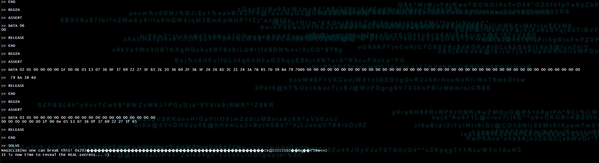
The working pattern so far is a grouped exchange using BEGIN, ASSERT, one or more DATA commands, then RELEASE and END.
Once the right blocks were replayed, the board advanced to SOLVE and printed a real result.
We found the live interface by getting the board to talk back consistently and by matching the output to the gameplay text. That gave us a known good entry point. At first this was done with the serial adapter. With the CH340N identified on the board, the same serial path can also be reached through USB.
We found the flash mattered by combining two observations. First, the console referenced 0x10000. Second, the dumped flash image had one of its few non empty regions starting exactly at 0x010000.
That is too clean to ignore.
We found the structure by watching what repeated and what actually changed device state. Single commands by themselves were not enough. Ordered groups were.
The cleanest example is the progression from normal prompt state into the later SOLVE output after replaying the framed blocks.
These are the commands we have actually seen matter during progression.
BEGIN
ASSERT
DATA
RELEASE
END
SOLVE
Based on the current output, DATA appears to take a selector and a payload. We have already seen working traffic that looks like this.
DATA 06
DATA 02 01 00 00 00 00 1F 00 0E 05 13 07 36 0F 37 69 22 27 3F 65 2E 20 36 69 2F 3B 3F 24 26 61 2C 21 24 3A 7B 65 7D 39 6A 79 7D
DATA 03 01 00 00 00 00 00 00 00 00 00 00 00 00 00 00 00 00 00 00 00 00 00 1F 00 0E 05 13 07 36 0F 37 69 22 27 3F 65
We also saw trailing output blocks after one of the framed DATA 02 exchanges:
79 6A 38 4D
The currently proven framing pattern is this:
BEGIN
ASSERT
DATA ...
RELEASE
END
A simple example of the shape, not necessarily every byte, looks like this:
BEGIN
ASSERT
DATA 06
RELEASE
END

BEGIN
ASSERT
DATA 02 ...
RELEASE
END

BEGIN
ASSERT
DATA 03 ...
RELEASE
END
Repeating that with the right blocks is what got us to the visible SOLVE stage.
This is the important jump from the earlier report. We are not just seeing the intro anymore. We now have proof that the board advances when the right sequence is replayed.
>> SOLVE
MAGICLIB{No one can break this! 0x20} ...
It is now time to reveal the REAL secrets...
Some output after MAGICLIB is still partially garbled in the terminal capture, but the state transition itself is real.
In circuit reads were messy because the board wakes up and interferes on the flash bus. Off board dumping with the RT809HSE gave stable matching dumps.
0xFFIt looks like the MCU contains the parser and game logic, while the external flash holds small challenge blocks that get referenced by address and turned into the command material the serial side expects. The user facing path is clearly serial. That serial access can come from a direct adapter or from USB through the CH340N. The SWIO path still matters, but it is no longer the only promising route.
SOLVE output with better logging or capture